

中文

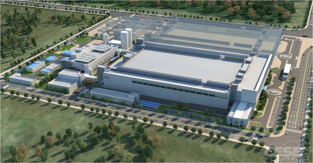
Hefei Nexchip Semiconductor Corporation 12-inch Production Line Project
Construction time: March 2016 - July 2017
Building area: 210,000㎡
Clean area: 30,000㎡
Cleanliness level: Class 10 - 1,000
Scope of contracting: MEP
Category:
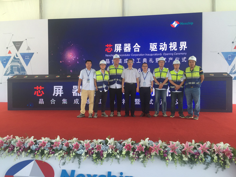
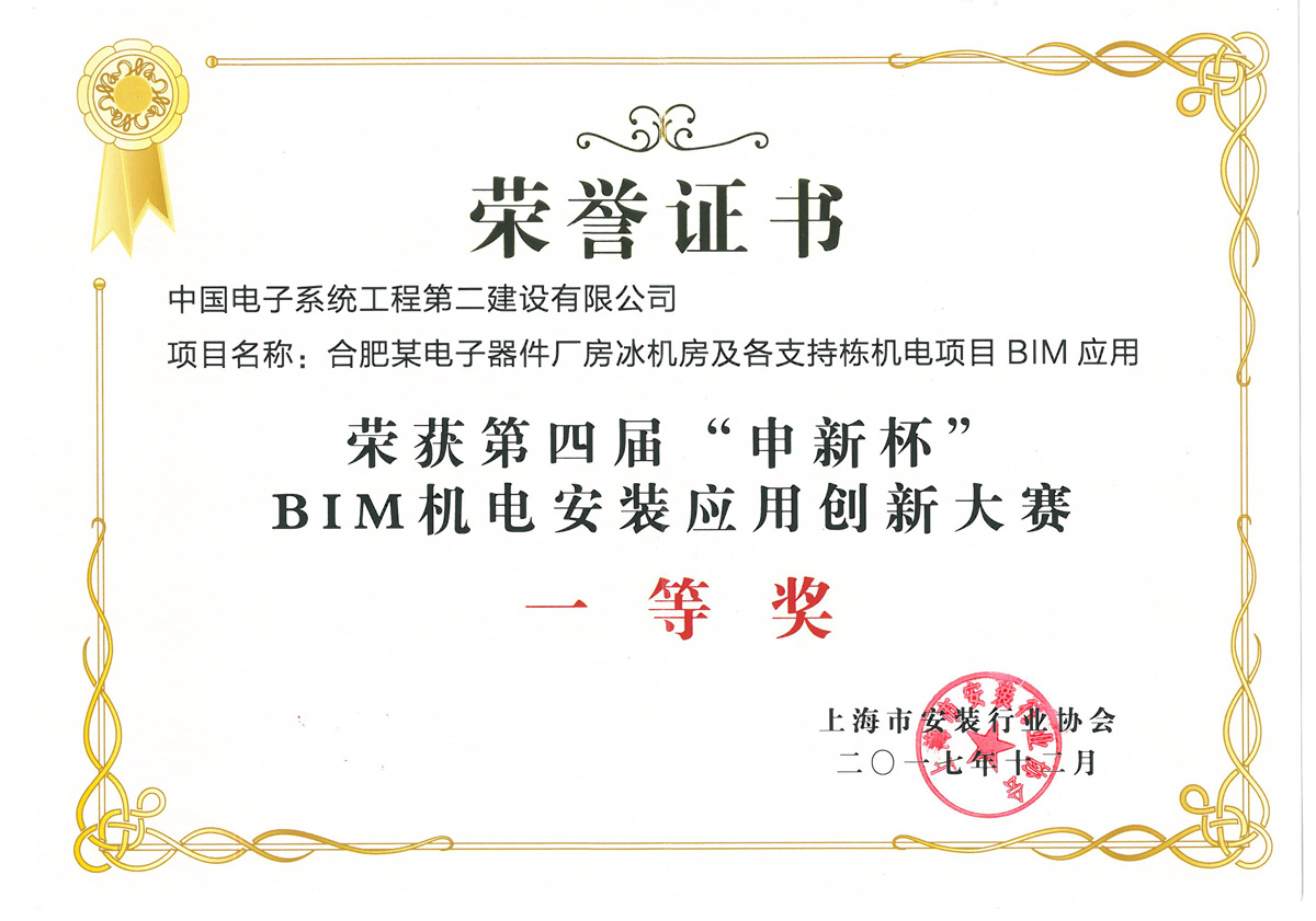
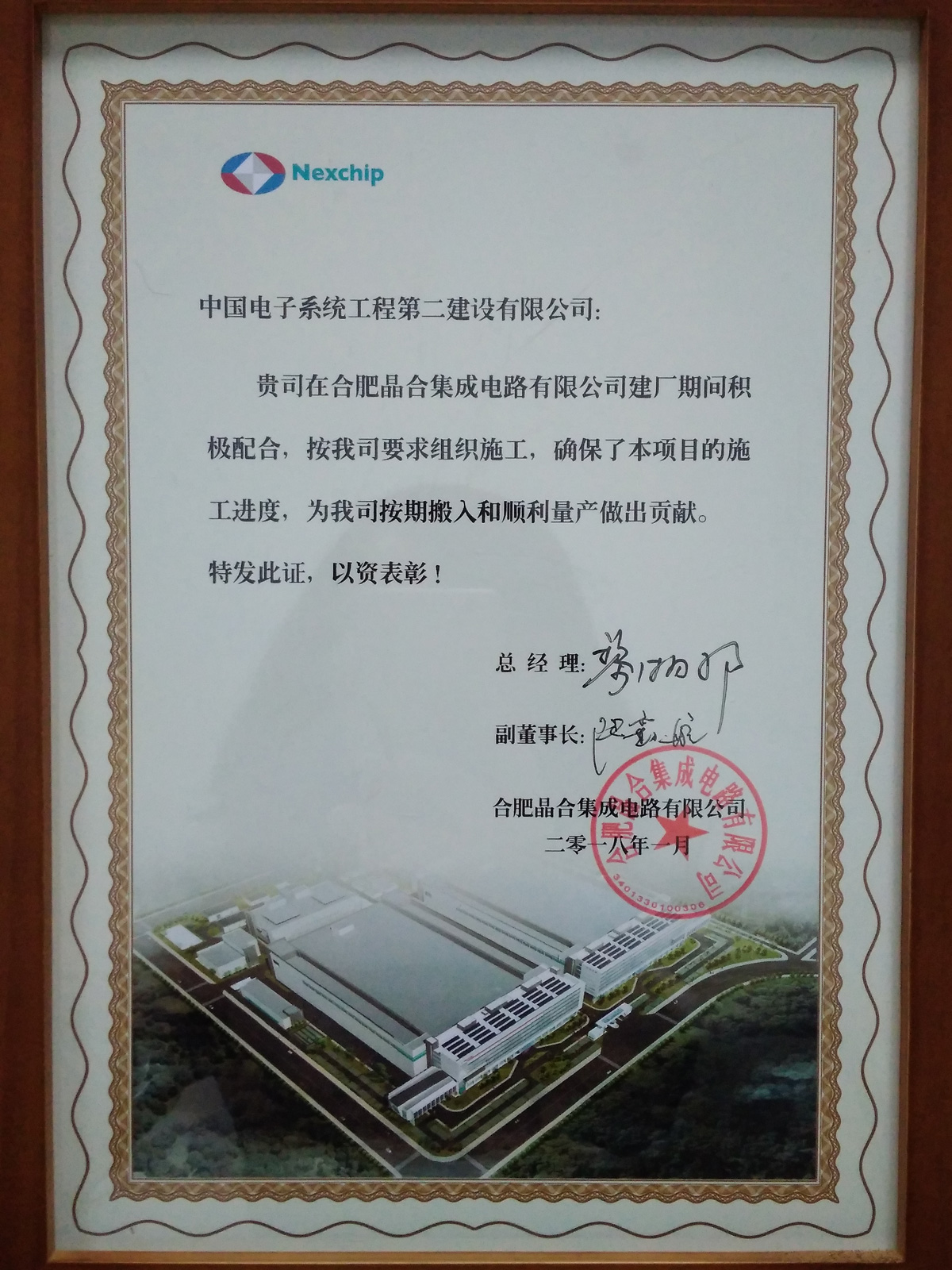
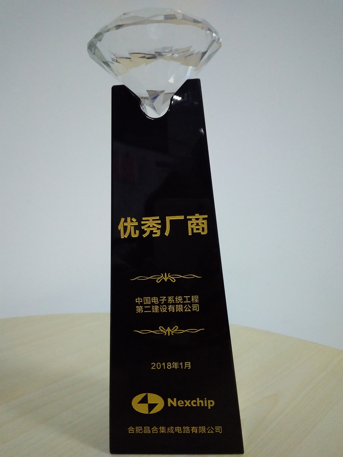
Project highlights: this project is a new 12-inch wafer foundry production line. The products are ICs of the display driver type, which mainly use 150nm technology to produce large-size display driver ICs, and use 110nm and 90nm technology to produce small and medium-size display driver ICs. The Hefei Nexchip Project is the first 12-inch integrated circuit production line in Anhui Province, and it is also the first 12-inch wafer foundry enterprise in China that focuses on the manufacturing of display driver chips; From laying a foundation to mass production, it only takes more than two years for Nexchip, and it only takes more than three months from trial production to the improvement of the "yield" that reached the parent company level, refreshing the construction speed of similar fabs.
|
|
| Aerial view |
|

Marketing Service Telephone
400 892 1298

Address: No.88,Juqu Road, Xinwu District, Wuxi City, Jiangsu Province
苏ICP备15056857号-1 Enterprise Post Office
COPYRIGHT©ALLRIGHTSRESERVED.China Electronics System Engineering No. 2 Construction Co., Ltd.
