

中文

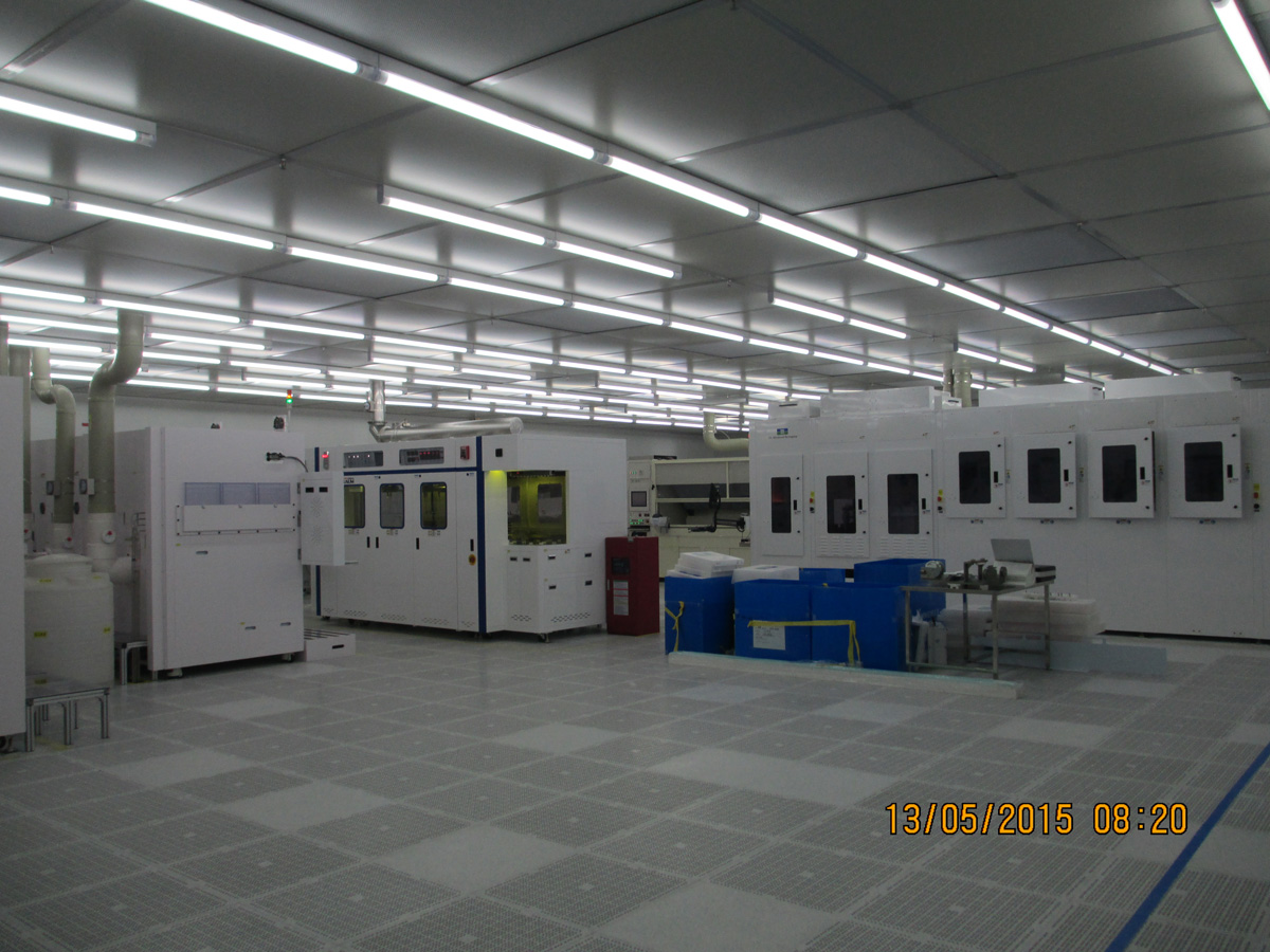
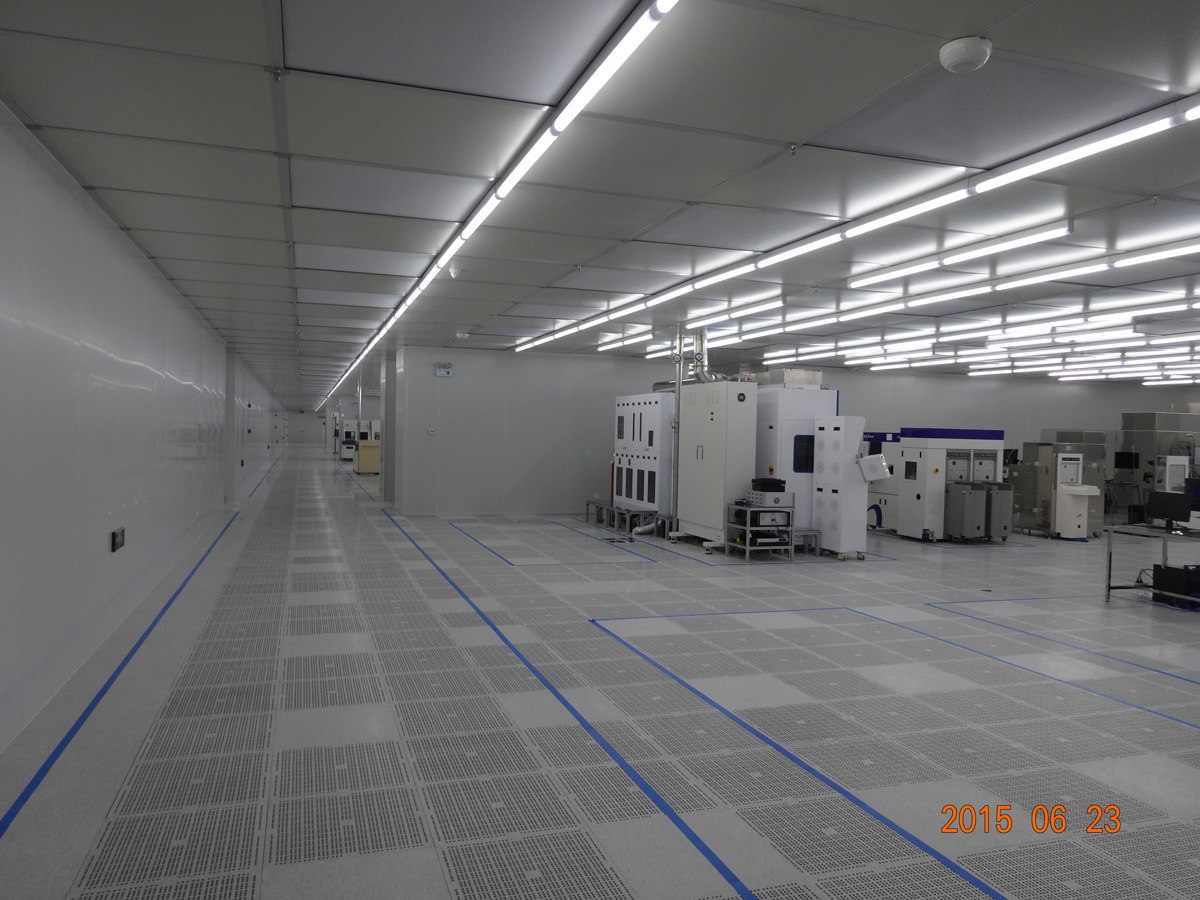
Nepes 1# Plant Dust-free Workshops
Construction time: January 2015 - June 2015
Building area: 11,000 (10,000㎡)
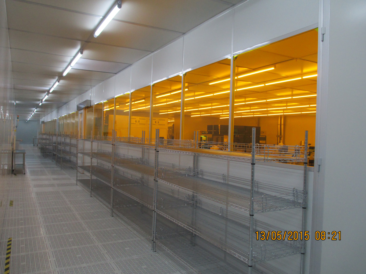
Clean area: 6,000 (10,000㎡)
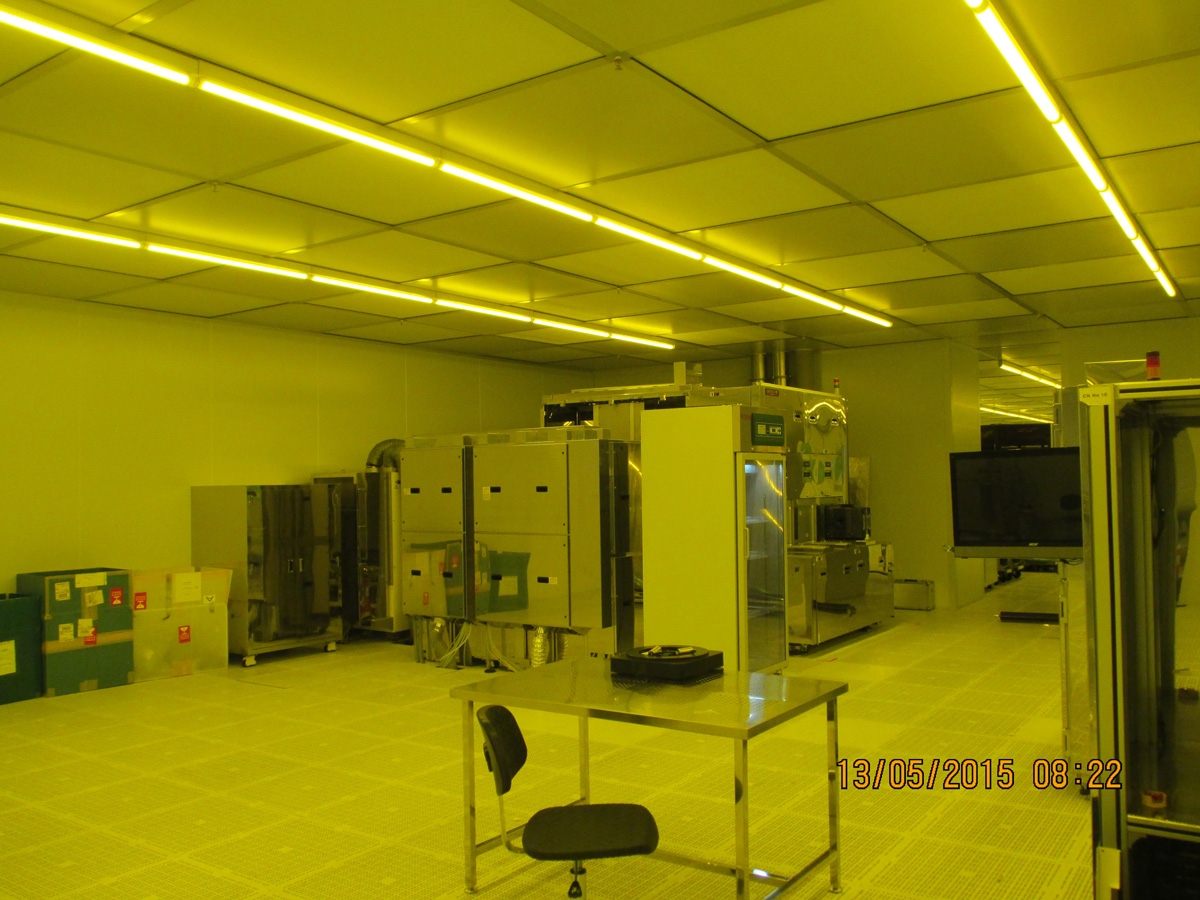
Cleanliness level: Class 100 - 1,000
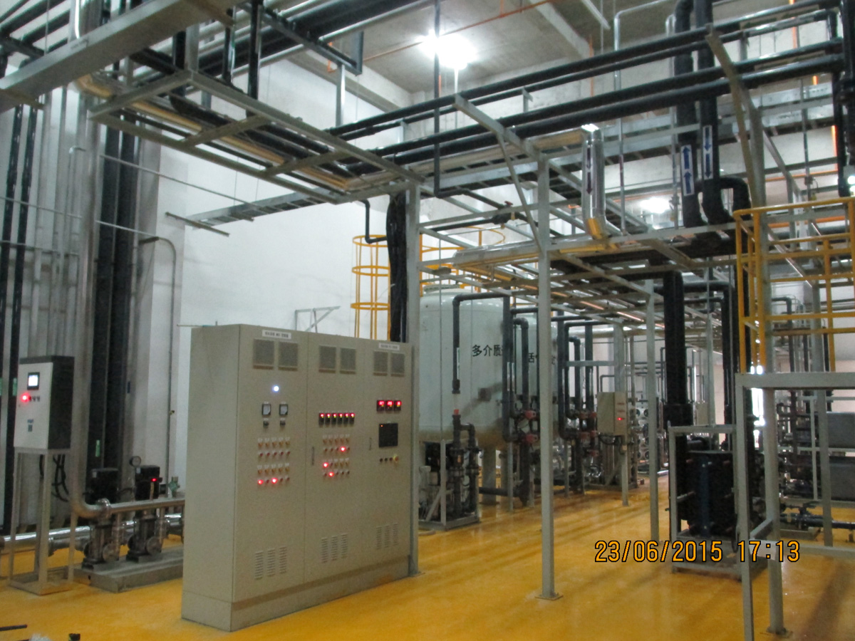
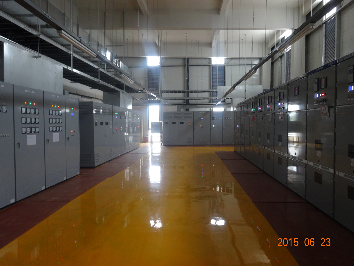
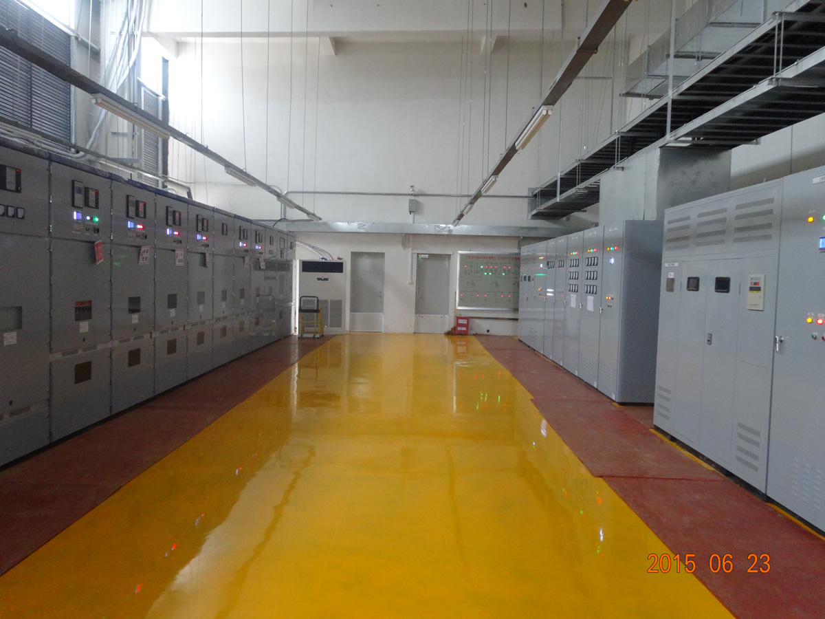
Scope of contracting: construction and electromechanical installation of dust-free workshops
Category:
Project highlights: The Company's Bumping technology has been widely used in fields such as core chip, power management chip, display driver chip, RF chip, camera chip, and fingerprint recognition system of portable mobile products. The wafer-level Bumping technology is becoming the mainstream application technology in sectors of high-end consumer electronics and industrial electronics.
 |
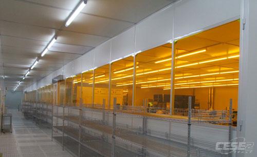 |
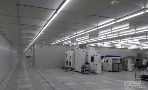
| ALive view of the project | Live view of the project |

Marketing Service Telephone
400 892 1298

Address: No.88,Juqu Road, Xinwu District, Wuxi City, Jiangsu Province
苏ICP备15056857号-1 Enterprise Post Office
COPYRIGHT©ALLRIGHTSRESERVED.China Electronics System Engineering No. 2 Construction Co., Ltd.
